
近1.5亿张照片! Intel Lunar Lake Processor超高定义内
发布时间:2025-05-19 09:54
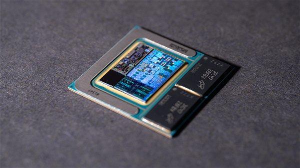 近1.5亿张照片! Intel Lunar Lake处理器超高定义内核许可证首次采用了许多创新技术! Lunar Lake是一代非常专业的Intel历史处理器,它采用了许多首次设计:主要的超命名,chiplet chiplet设计,TSMC铸造厂,包装,集成的NPU AI引擎和LPE超低功率小核心的组合记忆,而无需直接grasshopper。最近,专家Chip Fritzchens Fritz发布了一套高清的高清,这些定义是Lunar Lake处理器的关键图片,最大分辨率为近1.5亿个图片,显示了内部结构设计。 The computing module adopted the N3B process of TSMC, including four Leon Cove P Cores and their 2.5MB L2 cache per core, shared 12MB L3Cache, eight skymont e cores and their 4MB L2 cache per four sets, NPU AI engine (six groups of NCE neural network computing engines), XE2-LPG core graphics and media engines, memory memory, cache.我NTEL将几乎所有主要的计算模块都结合在一起,从而大大减少了彼此的通信延迟。平台控制器模块采用了TSMC N6工艺,该工艺主要负责各种高速和低速I/O,包括USB,Thunderbolt,PCIE,Bluetooth和Wi-Fi。还有一个填充模块,没有任何电路函数来维持整体形状和机械平衡。下面这些模块是基于Intel 22FFL过程的活动插音器,其中包括使用Intel Foveros 3D包装技术的所有组件。
 咨询电话:020-66888888 公司地址:广东省广州市番禺经济开发区 Copyright © 2024-2026 蘑菇吃瓜料每日爆料-蘑菇吃瓜官网黑料爆料-58爆料网每日精选最新消息 版权所有 备案号: |
 扫一扫,官方微信
|